MIT succeeds in rearranging 40,000 atoms within a solid crystal at room temperature/El MIT logra reorganizar 40.000 átomos dentro de un cristal sólido a temperatura ambiente
Source
A team from MIT (Massachusetts Institute of Technology) has achieved a fundamental breakthrough in materials engineering. They have developed a technique to "program" the position of tens of thousands of atoms within a solid crystal at room temperature and in a matter of minutes. This research represents a paradigm shift because it overcomes the limitations of previous techniques, which could only manipulate atoms on surfaces and under conditions of extreme cold—near absolute zero, or -273°C.
Un equipo del MIT (Massachusetts Institute of Technology) ha logrado un avance fundamental en la ingeniería de materiales. Han desarrollado una técnica para "programar" la posición de decenas de miles de átomos en el interior de un cristal sólido, a temperatura ambiente y en cuestión de minutos. Esta investigación representa un cambio de paradigma porque supera las limitaciones de las técnicas previas que solo podían manipular átomos sobre superficies y en condiciones de frío extremo cercanas al 0 absoluto o lo que es lo mismo -273 ºC.
Since 1989, atomic manipulation was limited to moving atoms across a material's surface. This required a vacuum and ultra-low temperatures. Furthermore, it was an extremely slow process—moving 35 atoms took hours—and impractical for creating actual devices. Using powerful microscopes at Oak Ridge National Laboratory, the MIT team has developed a sophisticated system of algorithms to control an electron beam with picometer precision (one-trillionth of a meter). In short, the researchers have created an atomic-scale "photocopier" capable of rewriting the interior of a material.
Desde 1989, la manipulación atómica se limitaba a mover átomos sobre la superficie de un material. Esto requería vacío y temperaturas ultrabajas. Además, era un proceso extremadamente lento (mover 35 átomos llevaba horas) y poco práctico para crear dispositivos reales. El equipo del MIT, utilizando potentes microscopios del Laboratorio Nacional Oak Ridge, ha desarrollado un sofisticado sistema de algoritmos para controlar un haz de electrones con una precisión de picómetros (una billonésima de metro). En pocas palabras, los investigadores han creado un "fotocopiador" a escala atómica capaz de reescribir el interior de un material.
Source
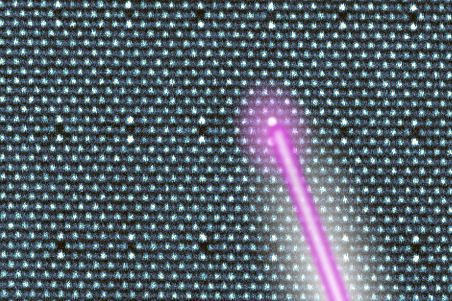
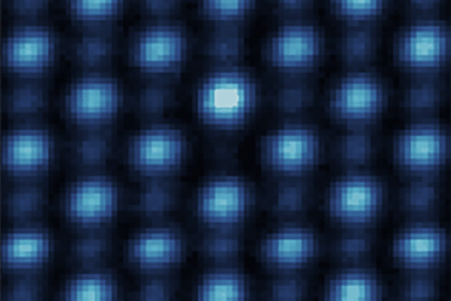
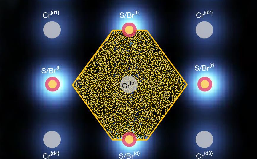
The electron beam performs a controlled oscillating motion that pushes entire columns of atoms into new positions within the crystal lattice. It is as if a row of atoms were "sliding" into a new location. This creates a pair of defects—a vacancy (the spot they leave behind) and an interstitial (the new spot they occupy)—and all of this occurs at room temperature. Using this technique, the team was able to create more than 40,000 of these quantum defects in a chromium sulfide-bromide crystal (only 13 nanometers thick) in approximately 40 minutes.
El haz de electrones realiza un movimiento oscilante diseñado que empuja columnas enteras de átomos a nuevas posiciones dentro de la red cristalina. Es como si se "deslizara" una fila de átomos a una nueva ubicación. Esto crea un par de defectos: una vacante (el lugar que dejan) y un intersticial (el nuevo lugar que ocupan) y todo esto sucede a temperatura ambiente. Con esta técnica, el equipo fue capaz de crear más de 40.000 de estos defectos cuánticos en un cristal de sulfuro-bromuro de cromo (de solo 13 nanómetros de grosor) en aproximadamente 40 minutos.
In the world of quantum physics, a "defect" in a crystal's structure is not necessarily a bad thing. On the contrary, a precisely created defect can be extraordinarily valuable, as it can act as a functional quantum component. This capability enables the design and creation of states of matter that do not exist in nature. By controlling the 3D arrangement of these defects, the material's electronic, magnetic, and optical properties can be "sculpted" at will. Since the defects are created within the crystal, they are shielded from the environment—making them far more stable than those created on the surface—thereby bringing them closer to real-world applications without the need for costly vacuum systems.
En el mundo de la física cuántica, un "defecto" en la estructura de un cristal no es necesariamente algo malo. Por el contrario, un defecto creado con precisión puede ser extraordinariamente valioso, ya que puede actuar como un componente cuántico funcional. Esta capacidad permite diseñar y crear estados de la materia que no existen en la naturaleza. Al controlar la disposición de estos defectos en 3D, se pueden "esculpir" las propiedades electrónicas, magnéticas y ópticas del material a voluntad. Dado que los defectos se crean en el interior del cristal, están protegidos del entorno lo que los hace mucho más estables que los creados en la superficie, acercándolos a aplicaciones en el mundo real sin necesidad de costosos sistemas de vacío.
Source
Although this technology is in its early stages and currently requires highly advanced electron microscopy equipment, its future implications are enormous, opening the door to what researchers call "programmable matter." The created defects can act as qubits (quantum bits) or as the interface between them. Being able to design their patterns in a controlled manner could pave the way for more robust and scalable quantum computers. Tiny sensors capable of detecting magnetic fields, electric fields, or temperatures at the atomic level could be manufactured, with applications in medicine, navigation, and materials exploration.
Aunque esta tecnología está en sus primeras etapas y actualmente requiere de equipos de microscopía electrónica muy avanzados, sus implicaciones a futuro son enormes y abren las puertas a lo que los investigadores llaman "materia programable". Los defectos creados pueden actuar como qubits (los bits cuánticos) o como la interfaz entre ellos. Poder diseñar sus patrones de forma controlada podría allanar el camino hacia ordenadores cuánticos más robustos y escalables. Se podrían fabricar sensores diminutos capaces de detectar campos magnéticos, campos eléctricos o temperaturas a nivel atómico, con aplicaciones en medicina, navegación y exploración de materiales.
The ability to create specific atomic patterns could revolutionize data storage, enabling the storage of massive amounts of information in incredibly small spaces. This breakthrough by MIT is a crucial step that makes "atom-by-atom 3D printing" a much more tangible goal. It is no longer a science fiction concept but an active field of research with real milestones. While a versatile atomic printer for home or industrial use is still years away, the first functional machines already exist, and the path is being paved toward what experts call "Manufacturing III"—the ability to print 3D objects atom by atom.
La capacidad de crear patrones atómicos específicos podría revolucionar el almacenamiento de datos, permitiendo guardar cantidades masivas de información en espacios increíblemente reducidos. El avance del MIT es un paso fundamental que convierte a la "impresión 3D átomo por átomo" en un objetivo mucho más tangible. Ya no es una idea de ciencia ficción, sino un campo de investigación activo con hitos reales. Aún faltan años para tener una impresora atómica versátil en casa o en la industria, pero ya tenemos las primeras máquinas funcionales y se está construyendo el camino hacia lo que los expertos llaman la Manufactura III, es decir, la capacidad de imprimir objetos en 3 dimensiones átomo a átomo.
More information/Más información
https://news.mit.edu/2026/researchers-reprogram-materials-quickly-rearranging-their-atoms-0513
Son tres avances sorprendentes de acuerdo a su impacto:
Gracias por compartir, saludos y éxitos..!
MIT made a nearly unbelievable leap towards manipulating 40,000 individual atoms of graphic track into a single crystal at 40 degrees Celsius (room temperature) in about 40 minutes. By precisely using electron beam technology and sophisticated algorithms, MIT was able to go beyond the limitations of manipulating atoms at absolute zero and the manipulation of only the surface of an atom when working with 3D printed crystals. Specifically, by producing stable 3D quantum defects, MIT has unlocked the potential for scalable quantum computing, massive amounts of data storage, and even 3D printing of all atoms, one at a time.